


This project was part of a lab assignment that walked us through the process of fabricating an array of MEMS heat actuators on silicon wafers. My teammates and I conducted several tests throughout the process. The details of the fabrication process and testing is described in the MEMS Fabrication and Testing Report, which can be downloaded here: [PDF]
In Short, I learned several cleanroom processes through this project. Some of these processes include: wet oxidation on silicon wafers; patterned sacrificial layering of photoresist with photolithography; performing electron beam evaporation to deposit metals; wet chemical etching (we etched aluminum); and how to remove sacrificial layers using an oxygen plasma asher.

Figure 1. No deflection at 0V. Tick mark:2.5um.

Figure 2. When 4V is applied on the heat actuator, it deflected 2um and at 10kHz it vibrated linearly. Tick mark:2.5um.

Figure 3. Zoomed on a single microactuator on the wafer. Tick mark:2.5um.

The wafer after RCA clean.

Wafer entering the furnace which is initially set to 250°C and then increased to 1000°C.

Measuring the thickness of the oxide layer using the Filmetrics F20 thin film measurement system.

The micromanipulator used to probe the devices on the wafer.

After successfully probing a single microactuator.

The heat actuator broke after applying 9V to it.

The SiO wafer after wet oxidation.

Exposing the wafer with the Suss mask aligner.

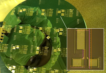
The resulting wafer after going through many fabrication process.